ice40_power
1.0.0
The goal of this exercise is to understand from a power point of view, what the various tradeoff's in the iCE40 FPGA are. This would allow us to design battery powered devices that use the FPGA and estimate battery life and also provide design time guidance.
Note: All currents in the table are in uA.
| Description | PLL (1.219V) | Bank 0 (3.283V) | Bank 1 (3.283V) | Bank 2 (3.283V) | Core (1.219V) |
|---|---|---|---|---|---|
| Unconfigured | 4.4 | 1.29 | 1552 | 1.5 | 381.6 |
| Reset | 4.4 | 1.29 | 82.9 | 1.5 | 188.3 |
| Blank design | 4.1 | 1.3 | 3.4 | 1.5 | 85.6 |
| External 12 MHz + 28 bit counter (32 LC's) | 4.1 | 1.3 | 3.4 | 1.5 | 613.5 |
| External 12 MHz + 28*2 bit counter (60 LC's) | 4.1 | 1.3 | 3.4 | 1.5 | 616.65 |
| External 12 MHz + 28*4 bit counter (116 LC's) | 4.1 | 1.3 | 3.4 | 1.5 | 624.2 |
| External 12 MHz + 28*8 bit counter (228 LC's) | 4.1 | 1.3 | 3.4 | 1.5 | 641.3 |
| HFOSC (48 MHz) + 24 bit counter (28 LC's) | 4.1 | 3.76 | 3.4 | 1.5 | 2184 |
| HFOSC (24 MHz) + 24 bit counter (28 LC's) | 4.1 | 3.76 | 3.4 | 1.5 | 1162 |
| HFOSC (12 MHz) + 24 bit counter (28 LC's) | 4.1 | 3.76 | 3.4 | 1.5 | 645 |
| HFOSC (6 MHz) + 24 bit counter (28 LC's) | 4.1 | 3.76 | 3.4 | 1.5 | 388.4 |
| LFOSC (10 kHz) + 24 bit counter (28 LC's) | 4.4 | 3.76 | 3.4 | 1.5 | 96.3 |
| External halted clock (0 kHz) + 24 bit counter (28 LC's) | 4.4 | 3.76 | 3.4 | 1.5 | 92.1 |
| HFOSC (12 MHz) + Math (no DSP) + 24 bit counter (208 LC's) | 4.1 | 3.76 | 3.4 | 1.5 | 996 |
| HFOSC (12 MHz) + Math (1 DSP) + 24 bit counter (72 LC's) | 4.1 | 3.76 | 3.4 | 1.5 | 882 |
| HFOSC + RGB (48 MHz clock) | 4.4 | 321.9 | 3.4 | 1.5 | 2195 |
| PLL (12MHz in, 16MHz output) | 138.6 | 1.29 | 3.42 | 1.4 | 1419 |
| PLL (12MHz in, 32MHz output) | 138.9 | 1.29 | 3.42 | 1.4 | 2029 |
| PLL (12MHz in, 48MHz output) | 103.6 | 1.29 | 3.42 | 1.4 | 2573 |
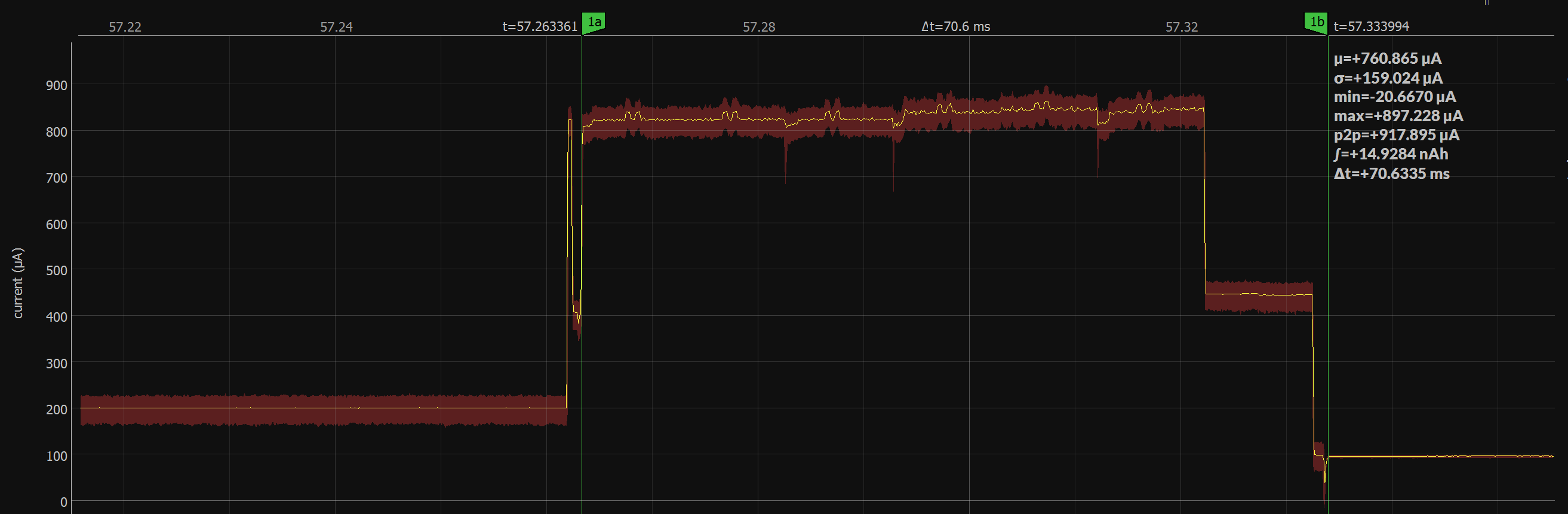
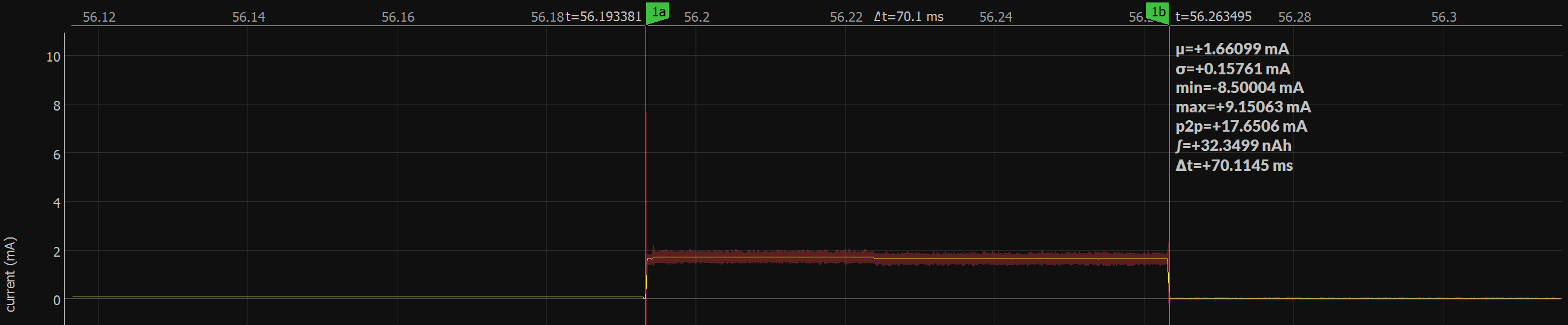
The FPGA boots from Flash programmed with low power 10kHz design. The FPGA configures itself from flash and draws power on the core and SPI flash bank (Bank 1) as shown below. The total energy consumption numbers as well as boot times are important for applications that will power off the FPGA and require it to boot up infrequently for power saving. As shown in the plots below, booting from the flash consumes about 46nAh of energy and takes about 70ms from start to finish. Note that this does not include the flash chip power consumption!
OK, great, now that we have measurements, what good is it if we cant use it! Lets start with a toy design so its easy to understand.
Clearly, we need to gate the clock on the FPGA when its asleep. Switching the design between 10kHz and 48MHz requires special care to avoid glitches on the clock when multiplexing between the two clocks. A Glitch free clock mux is a pretty standard component that does this cleanly.
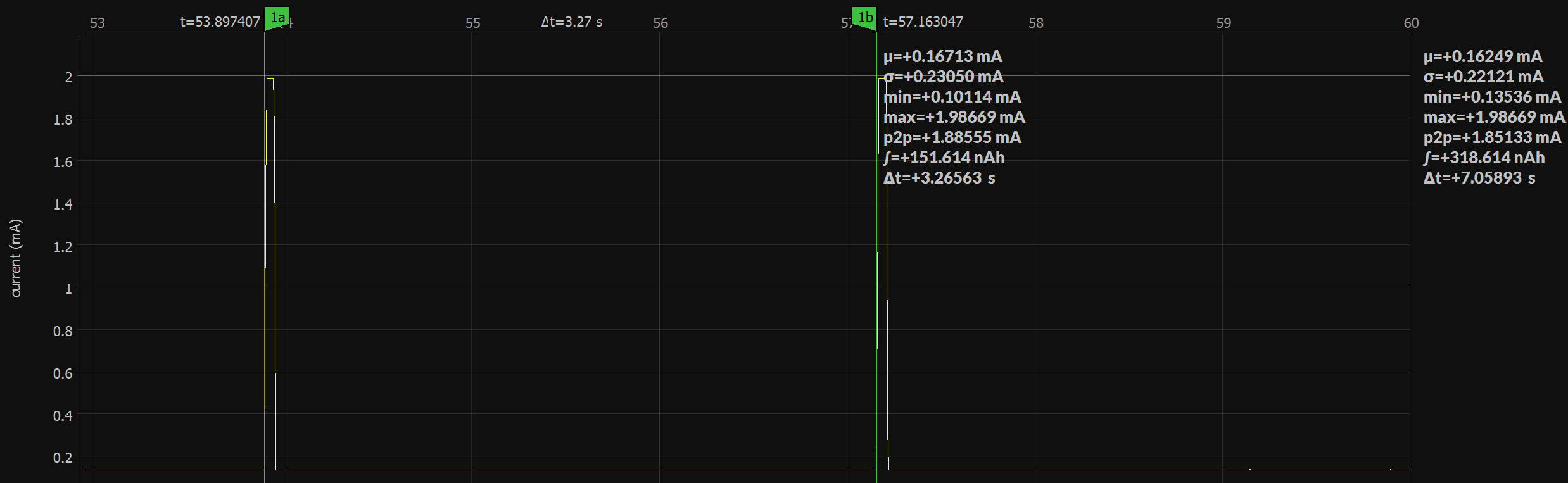
The 10kHz oscillator feeds not only the GFCM but also the timekeeper which switches the clock to the design that does the work. The timekeeper is a simple counter that selects the higher clock rate for 50ms every 3.2s.
The design that does the work in this case is a simple LED blinker and could be replaced by something quite complex.
A simple testbench was used to prove out the design and get rid of bugs...
The full design consumes 62 LC's, 3 SB_GB, 1 LF_OSC, 1 HF_OSC and the RGB driver. Heres the current consumption of the FPGA on the core power rail. As you can see, this seems to have achieved the goal!