PD PPS Controller
1.0.0
Interface for USB Type C Chargers with PD/PPS
This project originates in a colaboration with embres GmbH.
They did a great job in
There are some interesting boards out there to trigger USB Type C power delivery sources. Such as the ZY12PDN.
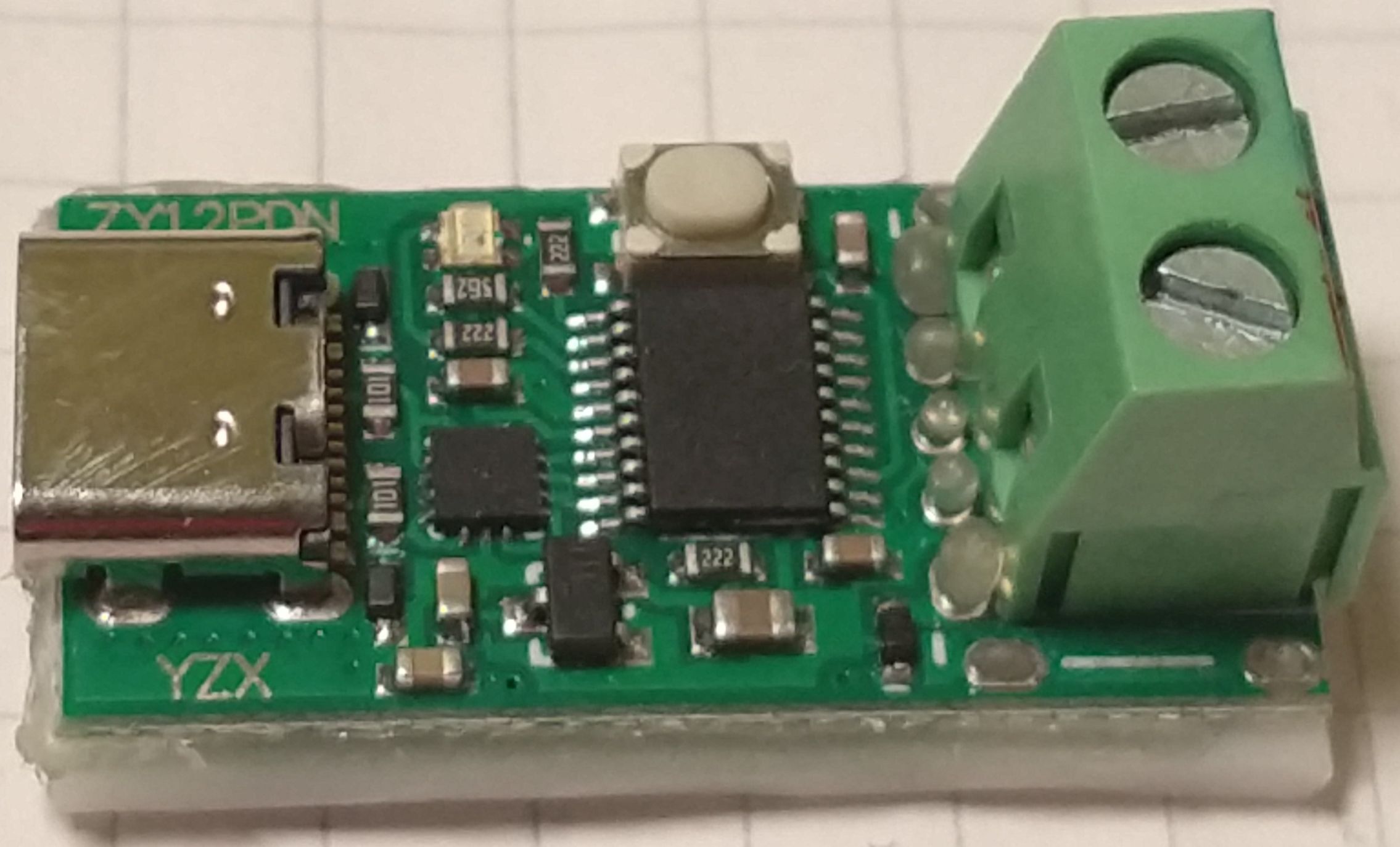
You can find many details at Manuel Bl.. These modules allow you to
step through the available fixed profiles which include 5 V, 9 V, 12 V, 15 V and 20 V.
There are many others out there, some have selectable voltage through resistors or jumpers.
I managed to get my hands on one the utilises a HUSB238 chip from Hynetek. This one
is programmable either through resistors or a microcontroller using I2C.
Unfortunatly this is well below the capabilities of a PD 3.0 compliant power supply. All these modules use only so called fixed profiles. But there is the PPS Mode (porgrammable power supply). This uses the augmented profile. The Augmented Profiles is spacified from 3.3 V to 21 V and up to 5 A. The voltage can be selected in 20 mV steps and the maximum current can be selected in 50 mA steps.
And here is my idea: Have you ever used one of those chunky lab power supplies eating up most space on your desk? These power supplies often range from 0 - 30 V and 0 - 5 A. As far as I am concerned, I mostly use 5 - 15 V at a few amps.
What if we can use this augmented profile to mimic a lab power supply? We would need a chip which is capable of
requesting this profile from a suitable PPS capable USB Type C power supply.
Well there is the easy and the hard way:
The easy way would be to tell some chip to request the desired voltage form the power supply.
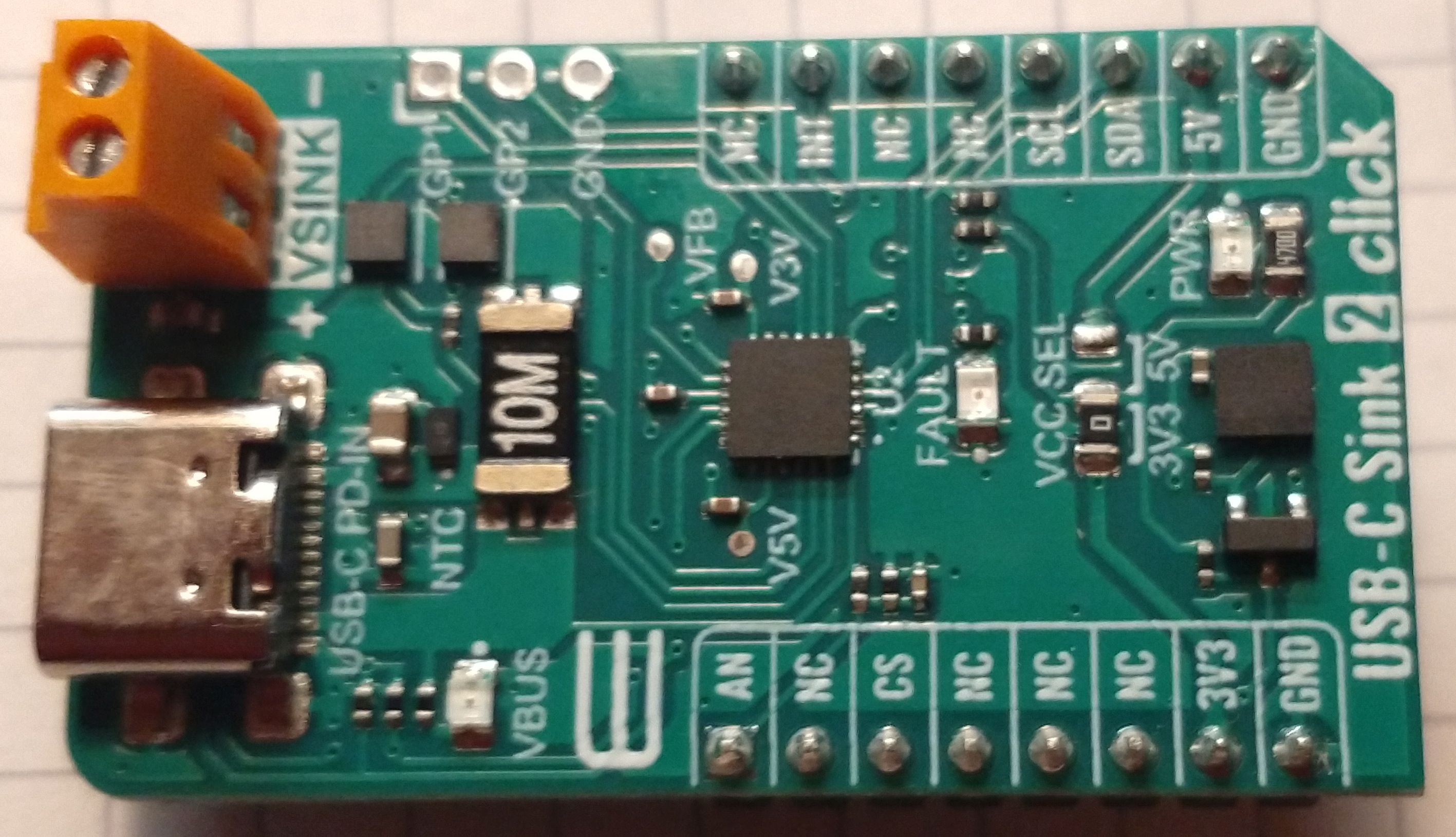
Such a chip is the AP33772 available from Diodes Incorporated. You can get a dedicated
evaluation board form Diodes or other manufacturers eg. MICROE. This is the
USB-C sink 2 click form MICROE:
This chip has been marked as NRND and was replaced by the AP33772S. The "S" version is even easier to use but has a huge
downside: It allows only 100 mV and 250 mA steps.
The hard way is to use one of those USB-C PD phys. they provide an OSI 0 + 1 interface to the power supply. Higher levels have to be implemented in SW. The most commonly used chip seems to be the FUSB302 form ON Semiconductor. This chip was used in the original ZY12PDN.
And here it is:
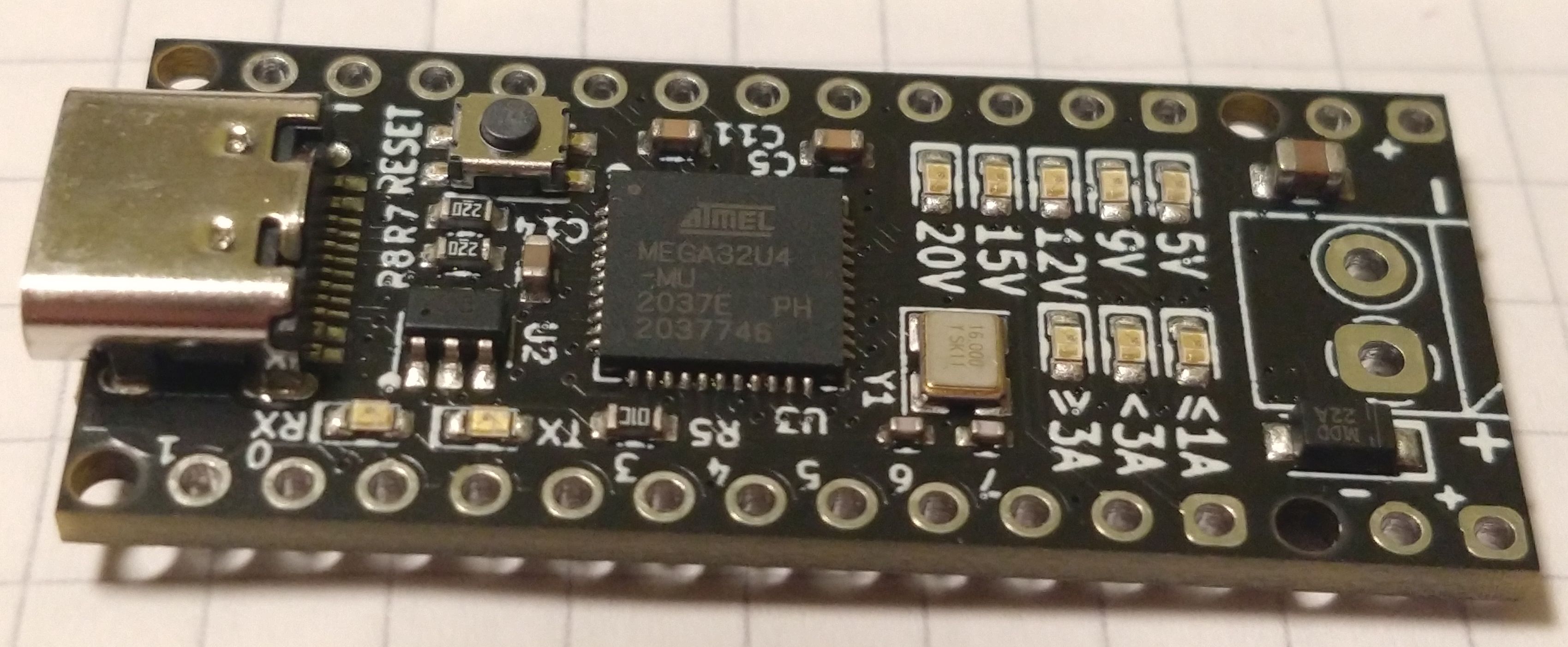
This is the PD-Micro deigned by Ryan Ma. It is Aruduino Pro Micro with
the FUSB302, some LEDs, a power switch and a voltage regulator. Ryan has made it easy to select appropiate
profiles. Kai Clemens Liebich has made some improvements to Ryan's
FUSB302 lib.
The only problem is voltage stability. Even when using 5 A USB C cables the voltage drop is quite significant.
So we might need to measure the output voltage to fine adjust the power supply voltage. The frist idea was to use
the internal ADC with an external 2.048 V voltage eference. The problem is, this is only a 10 bit ADC, but we need
to measure voltages up to 21 V. Assuming we clip at 20.48 V we will have a resolution of 20 mV. This seems to be
just enough but we can easyly do better. When using a dedicated ADC e.g. The INA219
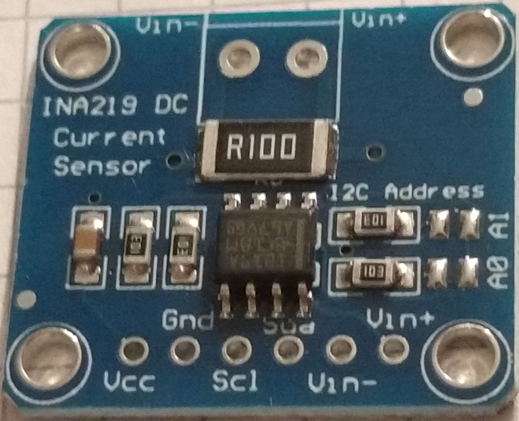
We can improve the precision to 4 mV. This is well below the 20 mV stepsize. An we get an current sensor on top.
Warning on current sensor ACS712
The ACS 712 is an easy to use isolated current sensor. But:
Now we can set a voltage, enable the output and measure the output voltage and current. So we can write a few lines of code to implement a constant voltage / current source. Well the reagulator response time will be limited by the speed of the power supply but it is within reasonable limits depenting on your USB power supply. My PS is an outdated Ugreen Nexode 2 with 100W which switches in ~40 .. 50 ms.
But how is the voltage and current slectet? Well we could use a serial interface and a computer to "remote control" the circuit. But what about an LCD a rotary switch as UI?.
And this leads me to my first prototype.
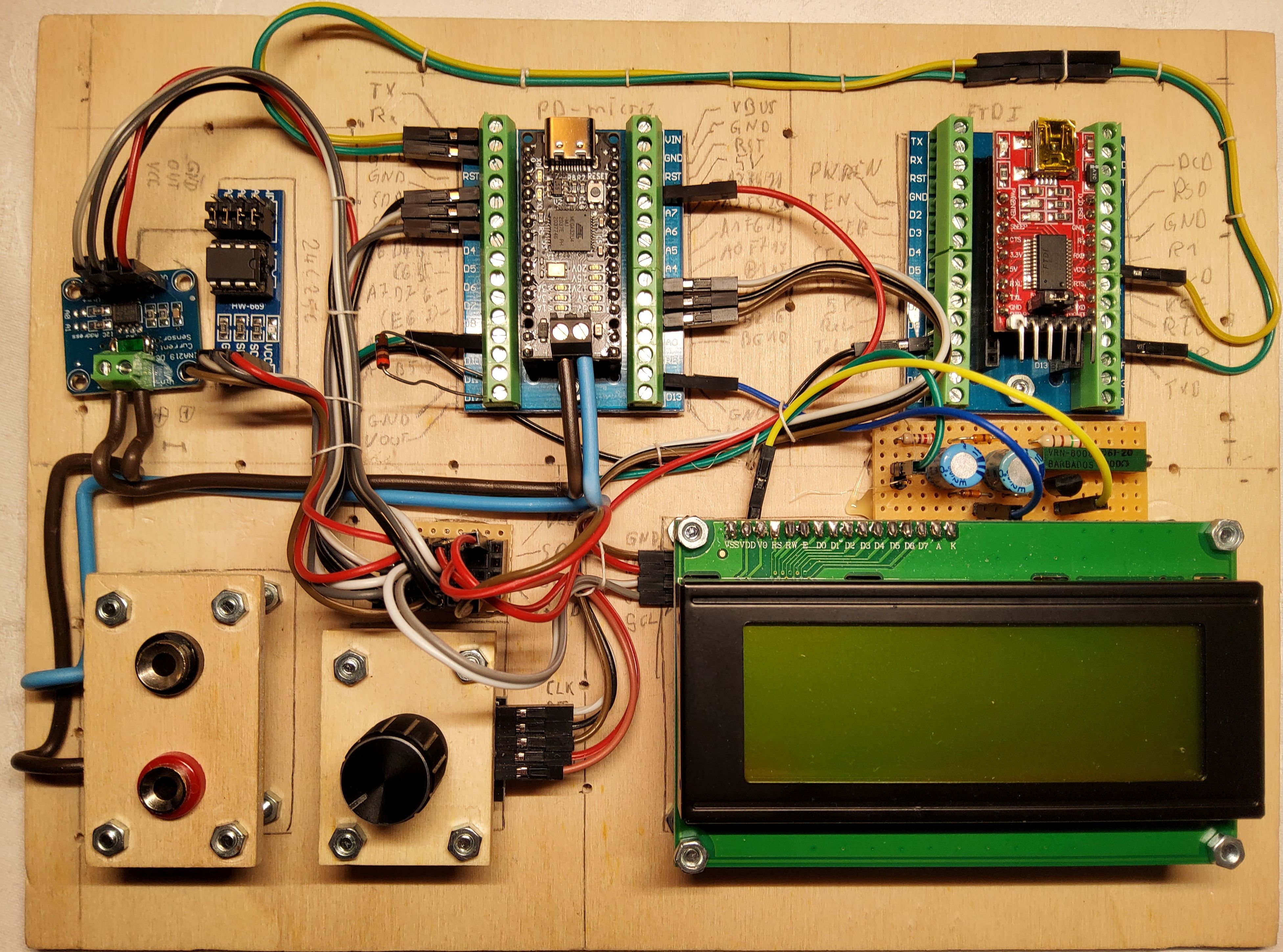
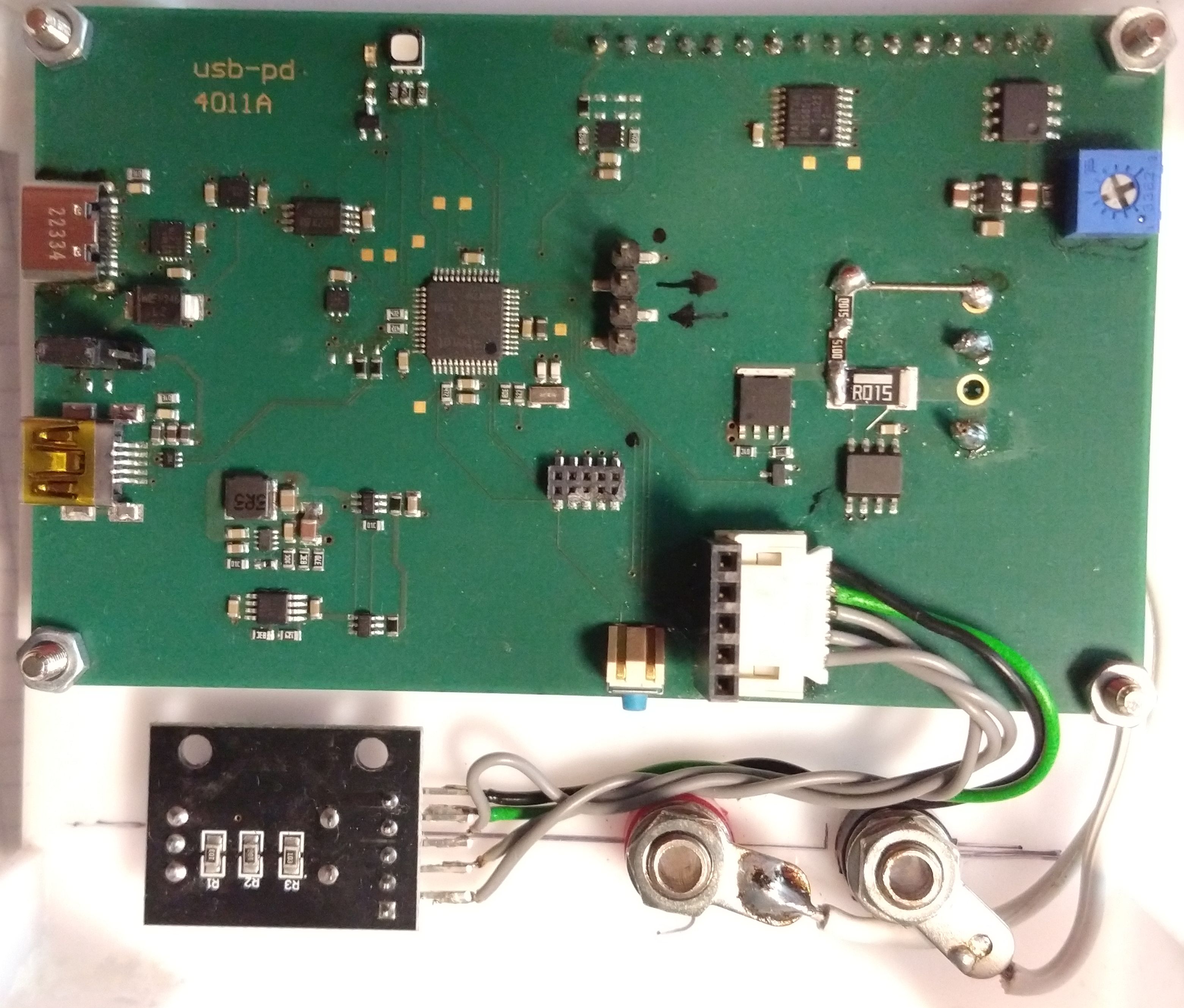
and here are the components clockwise beginnign with the upper left.
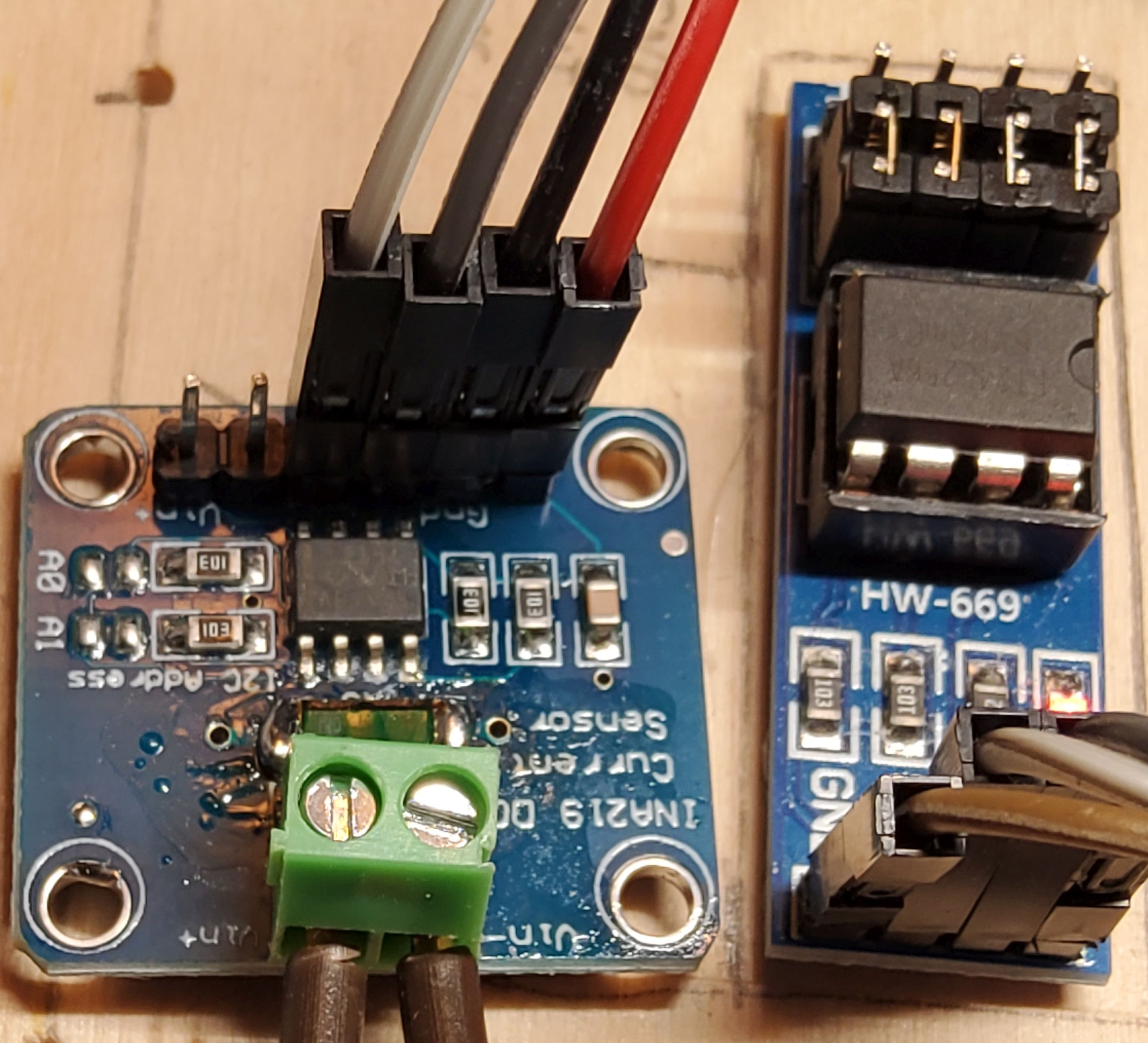
This is the voltage and current sensor. The shunt resistor has been reduced to R015 to get a 5 A full scale reading.
There is a serial EEPROM 24C256 on the board. This is used for parameter storage. I could have used the Atmel's on
chip EEPROM but this has way less wear resistance. I did not know how many write cycles would be needed, so i chose
an externel EEPROM
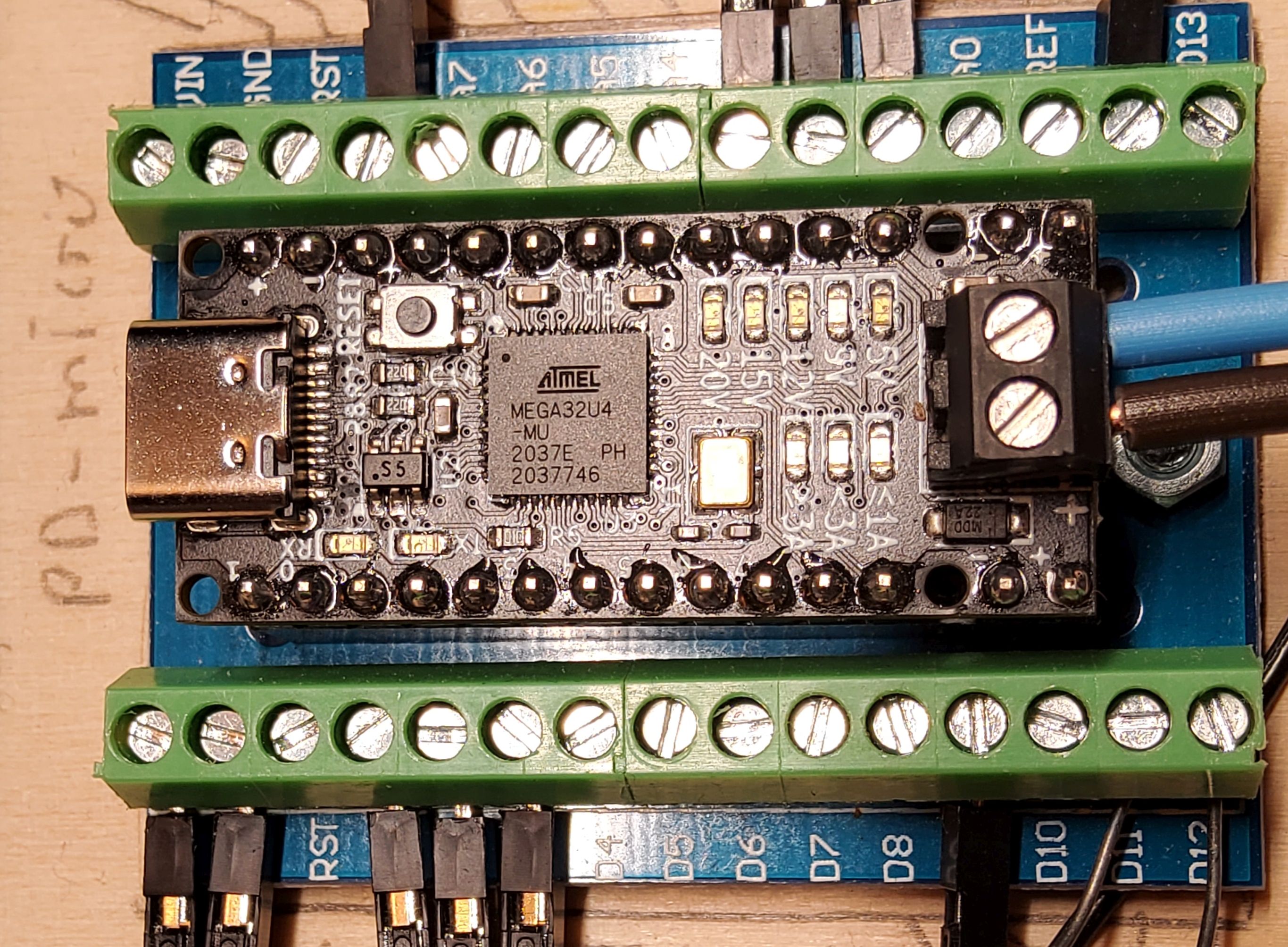
This is the heart of the circuit.
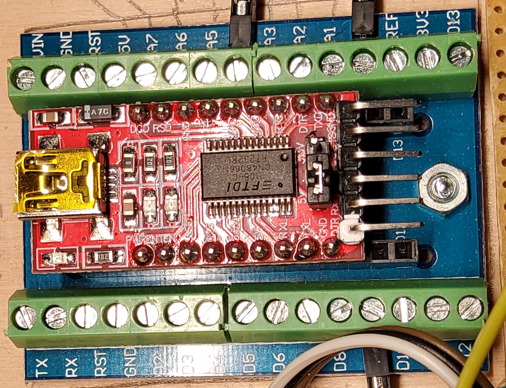 The USB - C port of the PD-Micro is occupied by the power supply. The USB interface can't be use for communication.
The HW serial interface is therefore wired to an FT232 USB to serial chip.
The USB - C port of the PD-Micro is occupied by the power supply. The USB interface can't be use for communication.
The HW serial interface is therefore wired to an FT232 USB to serial chip.
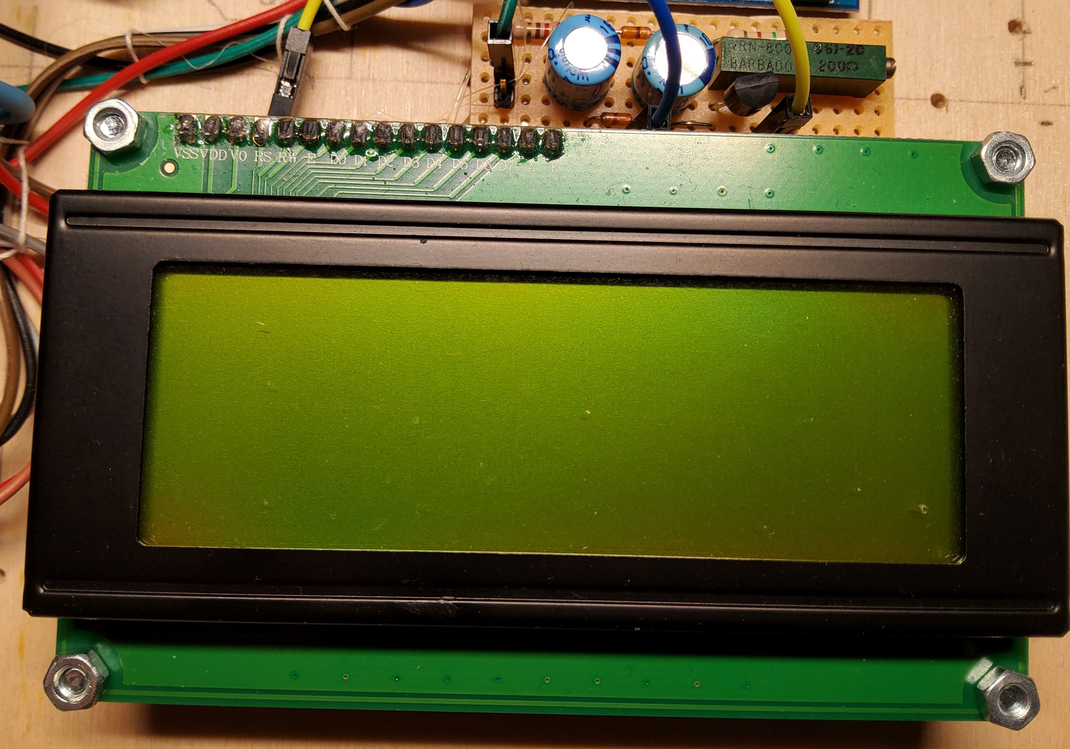
This is an 20x4 HD44780 compatible display with PCF8574, voltage inverter and current source for contrast as described
in my LCD library.
left to the display there is a KY-040 rotary encoder switch. Right above the switch there is just a I2C and VCC bus bar.
What features does a lab power supply need?


On startup the system will display a version and build message before starting in main menu.
 PD/PPS-Controller
====================
Ver. :   3.3 nbl
Build:   mmm dd yyyy
after initializiation is completed the main menu will be displayed
Mode (x:...) [UI^] !
     UU.UU V  I.II A
OUT  UU.UU V  I.II A
[i  i  i  i  i]  (i)
last line i: menu icons
to select a menu item press the button, a cursor will appear. Turn rotary switch until cursor is at the position of the desired item. Press button again to select the menu. In this menu the "V" and "A" in the second line are menu items too. Select to adjust desired voltage or current.
this menu is used to select the desired PD profile.
 # 1 / n  (...)
U= UU.UU V - UU.UU V
I=  I.II A max
[i  i  i]        (i)
last line i: menu icons
to select a profile press the button navigate to the "#" symbol in the first line and press again to enter profile selection. Turning will step through avalabla profiles. To select a profile press again and navigate to the check mark in the buttom line or select "x" to abort.
This menu is used to change the operation mode or calibration value.
(i)=auto  (*)=.    *
(i)=auto
(i)=auto
[i  i  i  x]     (i)
[i] or (i) icons in brackets
I= I.III A:  I.III A


[i  i  i  x]     (i)
[i] or (i) icons in brackets
to adjust the current measurment calibration enable output with a load and use a calibrated ampere meter to measure the current.
enter the settings menu and go to the calibration menu. enter the measured current and select the checkmark
it is reccommended to chose a current as high as possible to gain maximum precision.
the AVR SW is written with Arduino IDE. While developing the SW I found out a few things about the system:
after initial succes a quickly ran into issues with FLASH and RAM. You might be able to run the AVR code but I recommend to reduce the functionality the free some memory.
and this leads me to rhe second prototype using ATSAMD21G18.
The software in the AVR folder is as is. Ther will be no further development in this branch. It kind of work but use at your own risk. It only compiles without bootloader, you will need to add the boards.local.txt file from the config folder to
C:Users_user_AppDataLocalArduino15packagesarduinohardwareavr1.8.6
(at least on windows machines) and select Arduino Leonardo w/o bootloader from the available boards.
You will need AVRDUDE and an USBasp
Hint: be careful when purchasing one of the cheap clones. They often come with outdated SW and will not work.
It is no problem to update those but you will need a working USBasp adaptor.
programmer to flash the SW. For non cli users: AVRDUESS is a great gui for AVRDUDE.
You might as well use an Arduino Uno as USB to ISP bridge.
After my setbacks I tried an Arduino Zero. This board uses the ATSAMD21G18 which is a Cortex M0+ ARM controller running at 48 MHz. It has 256 kB FLASH and 32 kB RAM and lots of interfaces. A quick port showed that the SW could be easyly ported from AVR to ARM with almost no issues.
This was the point where we decided to start our first custom PCB avoiding all the problems encountered with the first portotype.
some headache cause the Vcc supply. Most buck converter circuits need some voltage headroom to operate and "feature" an
undervoltage lockout circuit. But this is a no go for this circuit. It needs to operate to as low as 3.3 V Vbus. We need an
undervoltage bypass curcuit to guarantee operation at 3.3 V Vbus. Otherwise the circuit would lock out when VBUS drops below the
thresholt which is typically 4 V - 4.7 V at 3.3 V output.
This problem was solved slightly overengineered. We used two 3.3 V regulators which are ored by to ideal diodes.
The TPS62932 is configured to output 3.45 V. The UVLO is set to 4.55 V and the Enable is set to 5.06 V. This guarantees
the buck converter operate above 5 V and outputs slightly above 3.3 V so the 3.3 V LDO is disabled savely. The LDO is a
NCV2951ACDMR2G set to 3.3 V. The dropout voltage is max 450 mV at 100 mA. The current consumption of the circuit is below 50 mA
so we will have an estimated max dropout of 300 mV.
When the input Voltage is above 5.06 V the LDO is idle and the Vcc is 3.45 V. When the input voltag drops below 4.55 V the buck
converter is disabled and the LDO takes ove, resulting in a Vcc of 3.3 V. When the input voltoge continues to fall, Vcc will
drop to ~3 V at 3.3 V Vbus.
The CPU will savely operate down to 2.7 V depending on the brownout settings.
The PCBA:
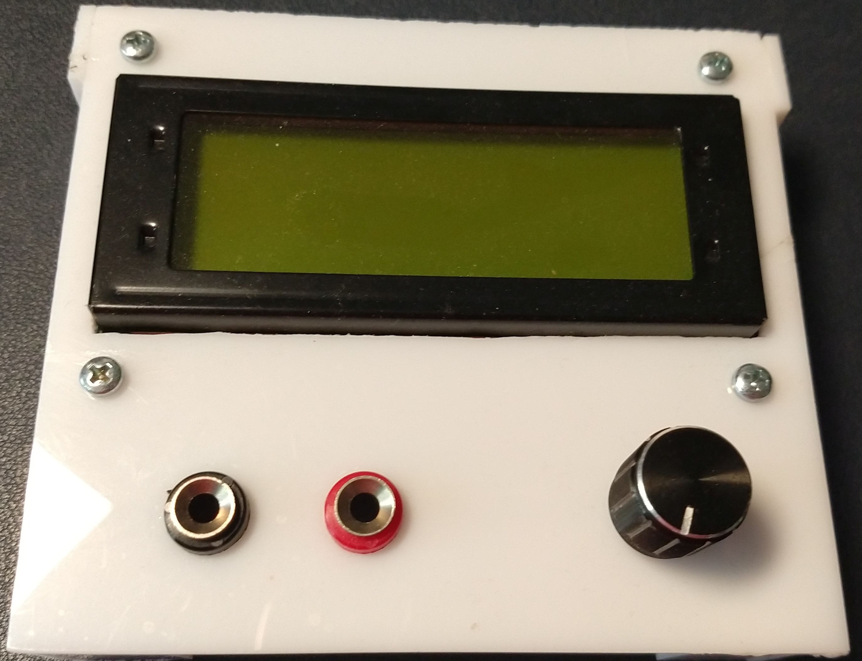
A working prototype:
Current Calibration
 internal   I.III A
 reference  I.III A
[i  i  i  x]     (i)
the current reading and the reference value have been reorganised.
The SW has been refactored and is now USB-PD2.
in the first SW the control of the power supply was implemente in the menu class. This is been moved to its own controller class.
A header for TODO reminders has been added
A power supply test class has been added to test profile changes.
In order to flash the SW for the first time you will need A JTAG Debug Interface such as
You can use Atmel Studio or the Arduino IDE to flash the Arduio Zero bootloader.
You can use the Blink Demo as well. Select Sketch -> export binary. The IDE will create a file xxx.ino.with_bootloader.arduino_zero.bin.
Just flash the file. You might need to copy the fuse bits from an Arduino Zero.
There are some samples in the Fuses folder. Some of the fuses are factory tuned and can not be overwritten.
Once the bootloader works you can flash SW using the SAM-BA bootloader. The SW provided by Microchip has a cli which is suitable for all SAM devices supporting SAM-BA and is therefore a bit tricky to use. A much more simple tool is Bossa from Shumatech.
My Charger supports 5 V / 9 V / 12 V / 15 V @ 3A and 20 V @ 5A fixed profiles and 3.3 V - 21 V @ 5 A augmented profile. Be careful many chargers marked with 100W (even Ugreen) will only support 65 W PPS (3.25 A) with limited voltage range. They may not supprot voltages below 3.3 V. Some will even have two PPS profiles with differnet voltage / current ratings.
UGREEN Nexode 2 Port 100W PD-Charger (Model CD254 #50827) Supported Profiles:
UGREEN Nexode 100W Desktop Charger (Model CD328 #90928) Supported Profiles:
Anker PowerPort I 30W PD
Supported Profiles:
iLepo USB C Fast Charger 65 W
Supported Profiles
INIU Power Bank 20000mAh, 22.5W
Supported Profiles
Some power suplly seem to reset the power when no current is drawn.
My "Nexode 100W Desktop Charger" P/N 90928 resets after ~1 h without load. Other chargers don't.
My INIU Power Bank resets with no load within ~10s
log with load 20R
0006: FUSB302 ver ID:B_revA
0118: USB attached CC1 vRd-3.0
0172: RX Src_Cap id=1 raw=0x53A1
0172:  obj0=0x2A01912C
0172:  obj1=0x0002D0E9
0172:  obj2=0x0003C096
0172:  obj3=0xC076323C
0172:  obj4=0xC0DC3228
0172:    [0] 5.00V 3.00A
0172:    [1] 9.00V 2.33A
0172:    [2] 12.00V 1.50A
0172:    [3] 5.00V-5.90V 3.00A PPS *
0172:    [4] 5.00V-11.00V 2.00A PPS
0176: TX Request id=0 raw=0x1082
0176:  obj0=0x42022628
0186: RX GoodCRC id=0 raw=0x0121
0192: RX Accept id=2 raw=0x05A3
0210: RX PS_RDY id=3 raw=0x07A6
0212: PPS 5.50V 2.00A supply ready
0214: Load SW ON
5214: TX Request id=1 raw=0x1282
5214:  obj0=0x42022628
5222: RX GoodCRC id=1 raw=0x0321
5228: RX Accept id=4 raw=0x09A3
5246: RX PS_RDY id=5 raw=0x0BA6
5246: PPS 5.50V 2.00A supply ready
10248:TX Request id=2 raw=0x1482
10248: obj0=0x42022628
10256:RX GoodCRC id=2 raw=0x0521
10262:RX Accept id=6 raw=0x0DA3
10280:RX PS_RDY id=7 raw=0x0FA6
10280:PPS 5.50V 2.00A supply ready
  ...
log without load:
0006: FUSB302 ver ID:B_revA
0118: USB attached CC1 vRd-3.0
0172: RX Src_Cap id=1 raw=0x53A1
0172:  obj0=0x2A01912C
0172:  obj1=0x0002D0E9
0172:  obj2=0x0003C096
0172:  obj3=0xC076323C
0172:  obj4=0xC0DC3228
0172:    [0] 5.00V 3.00A
0172:    [1] 9.00V 2.33A
0172:    [2] 12.00V 1.50A
0172:    [3] 5.00V-5.90V 3.00A PPS *
0172:    [4] 5.00V-11.00V 2.00A PPS
0176: TX Request id=0 raw=0x1082
0176:  obj0=0x42022628
0186: RX GoodCRC id=0 raw=0x0121
0192: RX Accept id=2 raw=0x05A3
0210: RX PS_RDY id=3 raw=0x07A6
0212: PPS 5.50V 2.00A supply ready
0214: Load SW ON
5214: TX Request id=1 raw=0x1282
5214:  obj0=0x42022628
5222: RX GoodCRC id=1 raw=0x0321
5228: RX Accept id=4 raw=0x09A3
5248: RX PS_RDY id=5 raw=0x0BA6
5248: PPS 5.50V 2.00A supply ready
10250:TX Request id=2 raw=0x1482
10250: obj0=0x42022628
10258:RX GoodCRC id=2 raw=0x0521
10264:RX Accept id=6 raw=0x0DA3
10284:RX PS_RDY id=7 raw=0x0FA6
10284:PPS 5.50V 2.00A supply ready

==> The Power bank resets and defaults to 5V only.

0006: FUSB302 ver ID:B_revA
0118: USB attached CC1 vRd-3.0
0352: TX Get_Src_Cap id=0 raw=0x0087
0704: TX Get_Src_Cap id=0 raw=0x0087
1056: TX Get_Src_Cap id=0 raw=0x0087